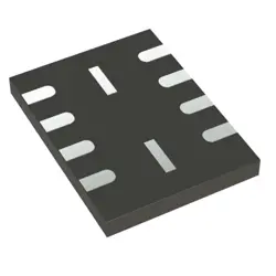
Изображения являются только для ссылки
74HCT259D
+БОМLatches 8-BIT ADDRSSBL LATCH
-
ПроизводительNexperia
-
Мфр. Часть #74HCT259D
-
В наличии23480
365 Дни гарантии качества
7*24 часы обслуживания каранти
90-гарантия послепродажного дня
Гарантия подлинного продукта
Спецификации
| Атрибут | Ценность |
| Standard Pack Qty | 50 |
Обзор
Description
The 74HCT259D is an 8-bit addressable latch from the HCT logic family, which is known for its high-speed CMOS technology combined with TTL compatibility. This device is typically used in applications requiring a latch with addressable and strobe capabilities. It features a single data input, eight latch outputs, and three address inputs, allowing one of the eight latches to be selected at a time. The 74HCT259D also includes a common reset pin that can clear all latches simultaneously.
Key characteristics of the 74HCT259D include its ability to directly interface with TTL devices due to its compatible input thresholds. It operates in a supply voltage range of 4.5V to 5.5V and is designed for high-speed operation, making it suitable for various digital storage and sequencing tasks. The device comes in a standard SOIC package, which supports easy integration into PCB designs. It is commonly employed in applications such as data distribution, demultiplexing, and memory address decoding.
Key characteristics of the 74HCT259D include its ability to directly interface with TTL devices due to its compatible input thresholds. It operates in a supply voltage range of 4.5V to 5.5V and is designed for high-speed operation, making it suitable for various digital storage and sequencing tasks. The device comes in a standard SOIC package, which supports easy integration into PCB designs. It is commonly employed in applications such as data distribution, demultiplexing, and memory address decoding.
Equivalent
The 74HCT259D is a high-speed CMOS 8-bit addressable latch. Equivalent products include the SN74HCT259N by Texas Instruments, MC74HC259 by ON Semiconductor, and CD74HCT259 by Texas Instruments. These alternatives offer similar functionality and electrical characteristics, making them suitable substitutes for applications requiring an 8-bit addressable latch. Always verify pin configurations and specifications to ensure compatibility with your specific application.
Features
The 74HCT259D is an 8-bit addressable latch with the following features:
1. High-Speed CMOS: It combines low power consumption with high speed.
2. Addressable Latches: It includes 8 latches that can be individually addressed through a 3-bit address.
3. Data Storage and Retrieval: The device can store and retrieve data via a common data input/output pin.
4. Latch Enable: A latch enable pin controls the latching operation, allowing data to be stored when active.
5. Reset Function: A master reset function is available to clear all latches simultaneously.
6. Wide Operating Voltage: It operates over a wide supply voltage range, typically 4.5 V to 5.5 V.
7. Low Power Consumption: The device is designed to minimize power use.
8. Compatibility: It is TTL-compatible, ensuring compatibility with other logic devices.
9. Compact Package: Typically available in small-outline packages like SOIC and TSSOP for space-efficient designs.
Overall, the 74HCT259D is suitable for applications requiring efficient data latching and selection.
1. High-Speed CMOS: It combines low power consumption with high speed.
2. Addressable Latches: It includes 8 latches that can be individually addressed through a 3-bit address.
3. Data Storage and Retrieval: The device can store and retrieve data via a common data input/output pin.
4. Latch Enable: A latch enable pin controls the latching operation, allowing data to be stored when active.
5. Reset Function: A master reset function is available to clear all latches simultaneously.
6. Wide Operating Voltage: It operates over a wide supply voltage range, typically 4.5 V to 5.5 V.
7. Low Power Consumption: The device is designed to minimize power use.
8. Compatibility: It is TTL-compatible, ensuring compatibility with other logic devices.
9. Compact Package: Typically available in small-outline packages like SOIC and TSSOP for space-efficient designs.
Overall, the 74HCT259D is suitable for applications requiring efficient data latching and selection.
Pinout
The 74HCT259D is a high-speed CMOS device that functions as an 8-bit addressable latch. It is commonly used in digital circuits for data storage and retrieval. This IC is part of the 74HCT series, which is known for its compatibility with TTL logic levels.
The 74HCT259D comes in a 16-pin dual in-line package (DIP) or small-outline integrated circuit (SOIC) package. The pin configuration is as follows:
1. VCC: Power supply pin.
2. GND: Ground pin.
3. D: Data input.
4. LE: Latch enable input.
5. CLR: Clear input (active low).
6. Q0-Q7: Outputs for each of the eight latches.
7. A0-A2: Address inputs to select which latch to write to.
8. E: Enable input.
The primary function of the 74HCT259D is to latch data from the input pin (D) into one of the eight outputs (Q0-Q7), based on the address inputs (A0-A2). The latch is enabled by the latch enable input (LE), and the outputs can be cleared using the CLR pin. This makes it useful in applications that require data storage and selection, such as memory addressing or simple data routing tasks.
The 74HCT259D comes in a 16-pin dual in-line package (DIP) or small-outline integrated circuit (SOIC) package. The pin configuration is as follows:
1. VCC: Power supply pin.
2. GND: Ground pin.
3. D: Data input.
4. LE: Latch enable input.
5. CLR: Clear input (active low).
6. Q0-Q7: Outputs for each of the eight latches.
7. A0-A2: Address inputs to select which latch to write to.
8. E: Enable input.
The primary function of the 74HCT259D is to latch data from the input pin (D) into one of the eight outputs (Q0-Q7), based on the address inputs (A0-A2). The latch is enabled by the latch enable input (LE), and the outputs can be cleared using the CLR pin. This makes it useful in applications that require data storage and selection, such as memory addressing or simple data routing tasks.
Manufacturer
The 74HCT259D is manufactured by Nexperia. Nexperia is a semiconductor company that specializes in producing discrete components, logic ICs, and MOSFETs. The company was established as an independent entity in 2017, originating from NXP Semiconductors’ Standard Products division. Nexperia focuses on efficiency in manufacturing and aims to deliver high-volume products to meet the demands of the automotive, industrial, computing, and consumer markets. Based in Nijmegen, Netherlands, Nexperia is known for its comprehensive portfolio of efficient power and signal conversion solutions.
Application
The 74HCT259D is a high-speed CMOS 8-bit addressable latch with applications in digital systems needing data storage and retrieval. It is commonly used in memory address decoding, where specific addresses need to be selected or controlled. The device serves well in applications requiring demultiplexing functions, enabling a single data input to be directed to multiple outputs. Additionally, it is suitable for implementing simple state machines and control systems within microcontrollers and programmable logic controllers (PLCs), and for managing output expansion in microprocessor systems. Its capability to drive LEDs or other low-power loads makes it versatile for various consumer electronics, industrial control systems, and communication equipment.
Package
The 74HCT259D is an integrated circuit featuring an 8-bit addressable latch with a 3-to-8 line decoder. Its package type is typically SOIC (Small Outline Integrated Circuit), which is a surface-mount package suitable for high-density board designs.