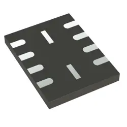
Изображения являются только для ссылки
74LVC595ABQ
+БОМ-
ПроизводительNexperia
-
Мфр. Часть #74LVC595ABQ
-
В наличии8436
365 Дни гарантии качества
7*24 часы обслуживания каранти
90-гарантия послепродажного дня
Гарантия подлинного продукта
Спецификации
| Атрибут | Ценность |
| Brand | Nexperia |
Обзор
Description
The 74LVC595ABQ is an 8-bit shift register IC with output latches and a serial input, designed for low-voltage applications (2.7V to 3.6V). It is part of the 74LVC family, which is known for its high-speed performance and low power consumption. This device can shift data in serially and latch it out in parallel, making it ideal for applications like LED control, data storage, and signal processing.
Key features include:
- 8-bit Shift Register: Allows for serial input and parallel output.
- Parallel Output Latch: Stores the shifted data for output.
- Low Voltage Operation: Compatible with logic levels from 2.7V to 3.6V.
- High-Speed Performance: Capable of operating at clock frequencies up to 100 MHz.
- Three-State Outputs: Enables easy interfacing with other digital circuits.
The 74LVC595ABQ is commonly used in microcontroller interfaces, LED drivers, and various digital communication applications, providing flexibility and efficiency in designing electronic systems.
Key features include:
- 8-bit Shift Register: Allows for serial input and parallel output.
- Parallel Output Latch: Stores the shifted data for output.
- Low Voltage Operation: Compatible with logic levels from 2.7V to 3.6V.
- High-Speed Performance: Capable of operating at clock frequencies up to 100 MHz.
- Three-State Outputs: Enables easy interfacing with other digital circuits.
The 74LVC595ABQ is commonly used in microcontroller interfaces, LED drivers, and various digital communication applications, providing flexibility and efficiency in designing electronic systems.
Equivalent
Equivalent products to the 74LVC595ABQ include the 74HC595 74HCT595, and 74LVT595. These chips serve similar functions as 8-bit shift registers with output latches. Ensure to check specifications like voltage levels and speed to confirm compatibility for your application.
Features
The 74LVC595ABQ is an 8-bit shift register featuring the following key characteristics:
1. 8-bit Shift Register: It can store and shift 8 bits of data serially.
2. Serial Input and Parallel Output: Data is input serially and can be output in parallel.
3. Low-Voltage Operation: Supports operation from 1.65V to 5.5V, making it suitable for low-power applications.
4. High-Speed Performance: Capable of operating at clock frequencies up to 100 MHz, offering fast data shifting.
5. Tri-State Outputs: Outputs can be placed in high-impedance state for flexible interfacing with other devices.
6. Built-in Latch Function: Allows the storage of the shifted data until it is needed, enabling controlled output.
7. Cascadable Design: Multiple devices can be connected for expanded shift register capabilities.
8. Low Power Consumption: Designed for energy-efficient applications.
9. TTL Compatible: Compatible with TTL logic levels for easy integration.
These features make the 74LVC595ABQ ideal for various digital applications, including LED control and data handling in microcontroller systems.
1. 8-bit Shift Register: It can store and shift 8 bits of data serially.
2. Serial Input and Parallel Output: Data is input serially and can be output in parallel.
3. Low-Voltage Operation: Supports operation from 1.65V to 5.5V, making it suitable for low-power applications.
4. High-Speed Performance: Capable of operating at clock frequencies up to 100 MHz, offering fast data shifting.
5. Tri-State Outputs: Outputs can be placed in high-impedance state for flexible interfacing with other devices.
6. Built-in Latch Function: Allows the storage of the shifted data until it is needed, enabling controlled output.
7. Cascadable Design: Multiple devices can be connected for expanded shift register capabilities.
8. Low Power Consumption: Designed for energy-efficient applications.
9. TTL Compatible: Compatible with TTL logic levels for easy integration.
These features make the 74LVC595ABQ ideal for various digital applications, including LED control and data handling in microcontroller systems.
Pinout
The 74LVC595ABQ is an 8-bit shift register with output latches and a serial interface. It has a total of 16 pins. Here’s a concise breakdown of its pin count and functions:
1. GND (Pin 1) - Ground.
2. Q7' (Pin 2) - Serial output for the last bit.
3. Q6 (Pin 3) - Output for bit 6.
4. Q5 (Pin 4) - Output for bit 5.
5. Q4 (Pin 5) - Output for bit 4.
6. Q3 (Pin 6) - Output for bit 3.
7. Q2 (Pin 7) - Output for bit 2.
8. Q1 (Pin 8) - Output for bit 1.
9. Q0 (Pin 9) - Output for bit 0.
10. SRCLK (Pin 10) - Shift register clock input.
11. RCLK (Pin 11) - Register clock input for latching.
12. SER (Pin 12) - Serial data input.
13. OE (Pin 13) - Output enable (active low).
14. MR (Pin 14) - Master reset (active low).
15. VCC (Pin 15) - Supply voltage.
16. NC (Pin 16) - No connection.
This device is widely used in digital circuits for controlling multiple outputs with a minimal number of pins.
1. GND (Pin 1) - Ground.
2. Q7' (Pin 2) - Serial output for the last bit.
3. Q6 (Pin 3) - Output for bit 6.
4. Q5 (Pin 4) - Output for bit 5.
5. Q4 (Pin 5) - Output for bit 4.
6. Q3 (Pin 6) - Output for bit 3.
7. Q2 (Pin 7) - Output for bit 2.
8. Q1 (Pin 8) - Output for bit 1.
9. Q0 (Pin 9) - Output for bit 0.
10. SRCLK (Pin 10) - Shift register clock input.
11. RCLK (Pin 11) - Register clock input for latching.
12. SER (Pin 12) - Serial data input.
13. OE (Pin 13) - Output enable (active low).
14. MR (Pin 14) - Master reset (active low).
15. VCC (Pin 15) - Supply voltage.
16. NC (Pin 16) - No connection.
This device is widely used in digital circuits for controlling multiple outputs with a minimal number of pins.
Manufacturer
The manufacturer of the 74LVC595ABQ is Texas Instruments (TI). Texas Instruments is a global technology company that designs and manufactures semiconductors and various integrated circuits. Founded in 1930, TI is known for its innovation in analog, digital signal processing, and microcontroller technologies, serving a wide range of industries including automotive, communications, consumer electronics, and industrial applications. TI's products are widely used in electronic systems and devices, making it one of the leading semiconductor companies worldwide.
Application
The 74LVC595ABQ is an 8-bit shift register with output latches, commonly used in digital circuits for various applications. Key areas include:
1. LED Drivers: Controlling multiple LEDs in displays and lighting systems.
2. Data Communication: Shifting data in serial-to-parallel conversion for communication protocols.
3. Microcontroller Interfaces: Expanding output capabilities of microcontrollers by driving more devices.
4. Signal Processing: Managing digital signals in sequential logic designs.
5. Automotive Systems: Implementing control systems in vehicles for features like lighting and sensors.
Its high-speed operation and low power consumption make it suitable for portable and battery-operated devices.
1. LED Drivers: Controlling multiple LEDs in displays and lighting systems.
2. Data Communication: Shifting data in serial-to-parallel conversion for communication protocols.
3. Microcontroller Interfaces: Expanding output capabilities of microcontrollers by driving more devices.
4. Signal Processing: Managing digital signals in sequential logic designs.
5. Automotive Systems: Implementing control systems in vehicles for features like lighting and sensors.
Its high-speed operation and low power consumption make it suitable for portable and battery-operated devices.
Package
The 74LVC595ABQ is typically offered in a TSSOP (Thin Shrink Small Outline Package) with 16 pins.