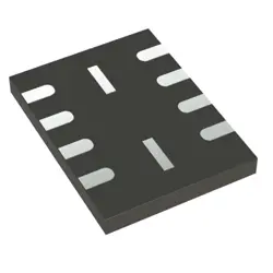
Изображения являются только для ссылки
FM25640B-G
+БОМIC FRAM 64KBIT SPI 20MHZ 8SOIC
-
Производителькорпорации Cypress Semiconductor Corp
-
Мфр. Часть #FM25640B-G
-
В наличии5311
365 Дни гарантии качества
7*24 часы обслуживания каранти
90-гарантия послепродажного дня
Гарантия подлинного продукта
Спецификации
| Атрибут | Ценность |
| Series | F-RAM™ |
| Part Status | Active |
| DigiKey Programmable | Not Verified |
| Memory Type | Non-Volatile |
| Memory Format | FRAM |
| Technology | FRAM (Ferroelectric RAM) |
| Memory Size | 64Kbit |
| Memory Organization | 8K x 8 |
| Memory Interface | SPI |
| Clock Frequency | 20 MHz |
| Voltage - Supply | 4.5V ~ 5.5V |
| Operating Temperature | -40°C ~ 85°C (TA) |
| Mounting Type | Surface Mount |
| Package / Case | 8-SOIC (0.154", 3.90mm Width) |
| Supplier Device Package | 8-SOIC |
Обзор
Description
The FM25640B-G is a non-volatile memory device from the FM series, specifically designed for applications requiring robust data storage. It features 64K bits (8KB) of memory, utilizing a ferroelectric technology that allows for high endurance and fast write cycles compared to traditional EEPROMs. This device retains data without needing power, making it suitable for battery-operated equipment and critical data logging applications.
Key features include a standard SPI interface for easy integration with microcontrollers, low power consumption, and wide operating temperature ranges. The FM25640B-G is ideal for automotive, industrial, and consumer electronics where reliability and data integrity are paramount. Additionally, it supports multiple write and read cycles, ensuring that users can access and store data efficiently.
Overall, the FM25640B-G offers a reliable solution for applications that require long-term data retention and fast access times, making it a versatile choice for engineers and developers.
Key features include a standard SPI interface for easy integration with microcontrollers, low power consumption, and wide operating temperature ranges. The FM25640B-G is ideal for automotive, industrial, and consumer electronics where reliability and data integrity are paramount. Additionally, it supports multiple write and read cycles, ensuring that users can access and store data efficiently.
Overall, the FM25640B-G offers a reliable solution for applications that require long-term data retention and fast access times, making it a versatile choice for engineers and developers.
Equivalent
The FM25640B-G chip is a 64K bit (8K x 8) ferroelectric RAM (FRAM) device. Equivalent products include the Cypress FM25L64B, Microchip M25P64, and STMicroelectronics M95640. Note that compatibility may vary based on specific application requirements, such as performance specifications and pin configurations. Always consult datasheets for detailed comparisons.
Features
The FM25640B-G is a non-volatile memory chip featuring 64Kb (kilobits) of ferroelectric RAM (FRAM). Key features include:
1. Fast Write Speed: It offers rapid write times, allowing for efficient data storage and retrieval.
2. Endurance: The device supports a high number of write cycles (up to 10 trillion), significantly surpassing traditional EEPROM or Flash memory.
3. Low Power Consumption: The FRAM technology ensures low energy usage during both read and write operations, making it suitable for battery-powered applications.
4. Wide Operating Voltage Range: The chip operates typically from 2.0V to 3.6V, providing flexibility for various applications.
5. Data Retention: It ensures data retention for over 10 years at room temperature.
6. Simple Interface: The chip supports a standard SPI (Serial Peripheral Interface) for easy integration.
7. Temperature Range: It is designed to operate in a broad temperature range, suitable for industrial applications.
These features make the FM25640B-G ideal for applications requiring fast, reliable, and energy-efficient non-volatile memory.
1. Fast Write Speed: It offers rapid write times, allowing for efficient data storage and retrieval.
2. Endurance: The device supports a high number of write cycles (up to 10 trillion), significantly surpassing traditional EEPROM or Flash memory.
3. Low Power Consumption: The FRAM technology ensures low energy usage during both read and write operations, making it suitable for battery-powered applications.
4. Wide Operating Voltage Range: The chip operates typically from 2.0V to 3.6V, providing flexibility for various applications.
5. Data Retention: It ensures data retention for over 10 years at room temperature.
6. Simple Interface: The chip supports a standard SPI (Serial Peripheral Interface) for easy integration.
7. Temperature Range: It is designed to operate in a broad temperature range, suitable for industrial applications.
These features make the FM25640B-G ideal for applications requiring fast, reliable, and energy-efficient non-volatile memory.
Pinout
The FM25640B-G is a 64Kb (8K x 8) ferroelectric RAM (FRAM) memory device. It features a total of 8 pins. The pin functions are as follows:
1. VDD: Power supply voltage.
2. GND: Ground.
3. SDA: Serial data line for data input/output.
4. SCL: Serial clock line for synchronizing data transfer.
5. HOLD: Hold pin to pause communication without losing data.
6. WP: Write protect pin to prevent accidental writes.
7. A0: Address pin used to select specific memory pages.
8. A1: Additional address pin for expanded memory addressing.
This component is designed for high endurance and low power consumption, making it suitable for various applications where data retention and speed are critical.
1. VDD: Power supply voltage.
2. GND: Ground.
3. SDA: Serial data line for data input/output.
4. SCL: Serial clock line for synchronizing data transfer.
5. HOLD: Hold pin to pause communication without losing data.
6. WP: Write protect pin to prevent accidental writes.
7. A0: Address pin used to select specific memory pages.
8. A1: Additional address pin for expanded memory addressing.
This component is designed for high endurance and low power consumption, making it suitable for various applications where data retention and speed are critical.
Manufacturer
The FM25640B-G is manufactured by Fusion-io, which is a part of Western Digital Corporation. Fusion-io specializes in flash memory products and solutions, focusing on enhancing data storage and performance for enterprise applications. Initially known for its innovative flash-based storage technology, the company has played a significant role in the evolution of memory solutions, particularly in high-performance computing environments.
Western Digital, the parent company, is a leading global data storage technology and solutions provider. It manufactures hard drives, solid-state drives, and storage systems for both consumer and enterprise markets. The FM25640B-G specifically is a non-volatile memory chip designed for applications requiring reliable data retention and quick access, making it suitable for various embedded systems and industrial applications.
Fusion-io’s expertise in flash memory and Western Digital’s extensive reach in storage technology underscore the importance of the FM25640B-G in modern computing solutions.
Western Digital, the parent company, is a leading global data storage technology and solutions provider. It manufactures hard drives, solid-state drives, and storage systems for both consumer and enterprise markets. The FM25640B-G specifically is a non-volatile memory chip designed for applications requiring reliable data retention and quick access, making it suitable for various embedded systems and industrial applications.
Fusion-io’s expertise in flash memory and Western Digital’s extensive reach in storage technology underscore the importance of the FM25640B-G in modern computing solutions.
Application
The FM25640B-G is a non-volatile memory device primarily used in various applications such as industrial automation, consumer electronics, and automotive systems. Key areas include firmware storage, data logging, configuration storage, and calibration data retention. Its ability to retain data without power makes it suitable for smart meters, medical devices, and IoT applications. Additionally, it serves in systems requiring frequent write cycles and reliable data integrity, enhancing overall performance in embedded systems and electronic devices.
Package
The FM25640B-G is typically available in a 32-pin SOIC (Small Outline Integrated Circuit) package. This package type is designed for surface-mount applications, offering a compact solution for integrating the memory chip onto circuit boards.