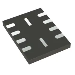
Изображения являются только для ссылки
LCMXO2-256ZE-1MG132C
+БОМIC FPGA 55 I/O 132CSBGA
-
Производителькорпорации Lattice Semiconductor Corporation
-
Мфр. Часть #LCMXO2-256ZE-1MG132C
-
Лист данных LCMXO2-256ZE-1MG132C DataSheet
-
Пакет CSBGA-132
-
В наличии4289
365 Дни гарантии качества
7*24 часы обслуживания каранти
90-гарантия послепродажного дня
Гарантия подлинного продукта
Спецификации
| Атрибут | Ценность |
| Package | Tray |
| Series | MachXO2 |
| ProductStatus | Active |
| NumberofLABs/CLBs | 32 |
| NumberofLogicElements/Cells | 256 |
| NumberofI/O | 55 |
| Voltage-Supply | 1.14V ~ 1.26V |
| MountingType | Surface Mount |
| OperatingTemperature | 0°C ~ 85°C (TJ) |
| Package/Case | 132-LFBGA, CSPBGA |
Обзор
Description
The LCMXO2-256ZE-1MG132C comes in a 132-pin Micro LED Package (MLP), providing a small footprint for space-constrained applications. It operates with a core voltage of 1.2 volts, optimizing power efficiency. The MachXO2 family includes embedded memory, PLLs for clock management, and support for various I/O standards, enhancing its versatility for different interfacing needs.
This FPGA is often used in consumer electronics, industrial automation, and communication systems. It is particularly valued for its instant-on capability, low power consumption, and robust security features, which include a unique device identifier and bitstream encryption options to protect intellectual property. Overall, the LCMXO2-256ZE-1MG132C is an ideal choice for developers looking to integrate programmable logic into compact and power-efficient designs.
Equivalent
Features
1. Logic Density: Contains 256 Look-Up Tables (LUTs).
2. Package: Comes in a 132-ball csBGA package.
3. Low Power Consumption: Offers a zero-power mode ideal for energy-efficient applications.
4. Non-volatile Technology: Instant-on capability with on-chip Flash memory.
5. I/O Options: Supports a variety of I/O standards, including LVCMOS, LVTTL, and more.
6. Embedded Memory: Equipped with embedded block RAM for on-chip data storage.
7. Clock Resources: Includes Phase-Locked Loops (PLLs) for clock management.
8. User Flash Memory: Integrated user Flash memory for additional data storage and configuration.
9. Security: Features security options for protecting design IP.
10. Programmability: Offers easy reprogrammability and design flexibility.
This component is suitable for a wide range of applications, including consumer electronics, industrial control, and communication systems, due to its compact size, low power usage, and versatile functionality.
Pinout
Key features and functions include:
1. Programmable Logic: It offers programmable logic blocks that can be configured for various digital logic functions.
2. Embedded Memory: Provides small amounts of embedded memory for data storage.
3. I/O Flexibility: Features a variety of I/O standards and provides flexible I/O pins for interfacing with other devices.
4. Low Power Consumption: Designed for low-power applications, making it suitable for portable and battery-operated devices.
5. Non-volatile Configuration Memory: Allows the FPGA to retain its configuration even after power-down.
The MachXO2 family FPGAs are often used in applications such as consumer electronics, industrial automation, and communication systems for tasks like glue logic, I/O expansion, and interface bridging.