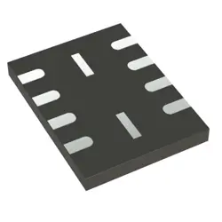
Изображения являются только для ссылки
MX25R1635FZUIH0
+БОМIC FLASH 16MBIT SPI/QUAD 8USON
-
ПроизводительМакроникс
-
Мфр. Часть #MX25R1635FZUIH0
-
Лист данных MX25R1635FZUIH0 DataSheet
-
В наличии1482
365 Дни гарантии качества
7*24 часы обслуживания каранти
90-гарантия послепродажного дня
Гарантия подлинного продукта
Спецификации
| Атрибут | Ценность |
| Series | MXSMIO™ |
| Part Status | Active |
| Base Product Number | MX25R1635 |
| DigiKey Programmable | Not Verified |
| Memory Type | Non-Volatile |
| Memory Format | FLASH |
| Technology | FLASH - NOR |
| Memory Size | 16Mbit |
| Memory Organization | 2M x 8 |
| Memory Interface | SPI - Quad I/O |
| Clock Frequency | 80 MHz |
| Write Cycle Time - Word, Page | 100µs, 4ms |
| Voltage - Supply | 1.65V ~ 3.6V |
| Operating Temperature | -40°C ~ 85°C (TA) |
| Mounting Type | Surface Mount |
| Package | 8-UFDFN Exposed Pad |
| Supplier Device Package | 8-USON (2x3) |
| Packaging | Cut Tape (CT), Tape & Reel (TR) |
Обзор
Description
This memory chip is known for its fast read performance, with a maximum clock frequency of up to 133 MHz, and supports various read modes, including Fast Read, Dual Output Fast Read, and Quad Output Fast Read. It also incorporates advanced security features such as block protection and a write protection mechanism to safeguard data integrity.
The MX25R1635FZUIH0 is housed in a compact 8-pin package, making it easy to integrate into space-constrained designs. Its reliability and endurance ensure a long operational life, making it an ideal choice for applications like IoT devices, consumer electronics, and industrial control systems.
Equivalent
1. Winbond W25Q16JV - 16Mb SPI NOR Flash.
2. Cypress S25FL116K - 16Mb SPI NOR Flash.
3. Micron M25P16 - 16Mb SPI NOR Flash.
4. Adesto AT25SF161 - 16Mb SPI NOR Flash.
When selecting, ensure compatibility with your specific application requirements.
Features
1. Low Power Consumption: It operates with low current, making it suitable for battery-powered applications.
2. Wide Temperature Range: Supports industrial temperature range from -40°C to +85°C.
3. Memory Organization: 2,097,152 bytes arranged in sectors and blocks for flexible data management.
4. Fast Read Performance: Supports various read modes, including fast read and dual/quad I/O for high-speed operation.
5. Low Voltage Operating Range: Works with a voltage range from 1.65V to 3.6V, optimizing for power efficiency.
6. Security Features: Includes hardware and software protection, with block protection and OTP (One-Time Programmable) regions.
7. Package Options: Available in compact packages suitable for space-constrained applications.
This Flash memory is ideal for portable and embedded systems requiring efficient data storage with low power usage.
Pinout
1. CS# (Chip Select): Activates the chip when low.
2. SCLK (Serial Clock): Provides the clock signal for data transfers.
3. SI (Serial Input)/IO0: Serial data input and output pin; used for commands and data input in SPI mode.
4. SO (Serial Output)/IO1: Serial data output pin; data is output through this pin in SPI mode.
5. WP# (Write Protect)/IO2: Provides hardware protection; can also be used as a data line in Quad I/O mode.
6. HOLD#/RESET#/IO3: Can hold the operation, reset the device, or serve as a data line in Quad I/O mode.
7. VCC: Power supply input.
8. VSS: Ground.
This chip supports standard, dual, and quad SPI modes, making it versatile for various applications needing non-volatile storage.
Manufacturer
Application
Package
Frequently Asked Questions
Q: What is the operating voltage range for the MX25R1635FZUIH0?
A: It operates from 1.65V to 3.6V, making it suitable for low-power and battery-powered applications.
Q: What is the maximum clock frequency supported by this NOR Flash?
A: The device supports a maximum SPI clock frequency of 80 MHz for high-speed data transfer.
Q: Is this component compatible with Quad I/O SPI interfaces?
A: Yes, it features a SPI - Quad I/O memory interface, enabling faster read and program operations.
Q: What is the memory organization of the MX25R1635FZUIH0?
A: It is organized as 2M x 8 bits, providing a total memory size of 16 Mbit.
Q: What are the typical write cycle times for this Flash memory?
A: Word write time is 100μs, and page write time is 4ms, ensuring efficient programming.
Q: What package type does this component use?
A: It comes in an 8-UFDFN Exposed Pad package, with a supplier device package of 8-USON (2x3mm).
Q: What temperature range can this device withstand?
A: The operating temperature range is -40°C to 85°C (TA), suitable for industrial environments.