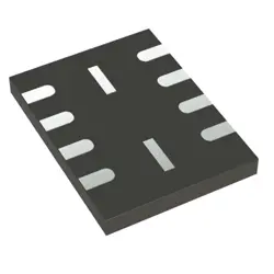
Изображения являются только для ссылки
SN74AC573PWR
+БОМIC OCT D-TYP TRNSP LATCH 20TSSOP
-
ПроизводительТехасские инструменты
-
Мфр. Часть #SN74AC573PWR
-
В наличии6672
365 Дни гарантии качества
7*24 часы обслуживания каранти
90-гарантия послепродажного дня
Гарантия подлинного продукта
Спецификации
| Атрибут | Ценность |
| Package | Tape & Reel (TR),Cut Tape (CT),Bulk |
| Series | 74AC |
| ProductStatus | Active |
| LogicType | D-Type Transparent Latch |
| Circuit | 8:8 |
| OutputType | Tri-State |
| Voltage-Supply | 2V ~ 6V |
| IndependentCircuits | 1 |
| DelayTime-Propagation | 2.5ns |
| Current-OutputHighLow | 24mA, 24mA |
| OperatingTemperature | -40°C ~ 85°C |
| MountingType | Surface Mount |
| Package/Case | 20-TSSOP (0.173, 4.40mm Width) |
Обзор
Description
The SN74AC573PWR is a high-speed, octal D-type transparent latch with 3-state outputs, manufactured by Texas Instruments. It is part of the Advanced CMOS (AC) logic family, which is known for its low power consumption and high performance. This device features eight latches that can store binary information, controlled by a latch-enable pin (LE). When the LE pin is high, data at the inputs (D0-D7) is latched, and when LE is low, the data is retained.
Output control is provided by the output enable (OE) pin, which, when high, places the outputs in a high-impedance state, allowing for bus line sharing without interference. With a supply voltage range of 2V to 6V, the SN74AC573PWR operates efficiently within a standard logic level environment. It is commonly used in applications requiring data storage, buffering, or data interfacing within microcontrollers, memory systems, or other digital systems. The device is available in a TSSOP package, which is suitable for space-constrained designs.
Output control is provided by the output enable (OE) pin, which, when high, places the outputs in a high-impedance state, allowing for bus line sharing without interference. With a supply voltage range of 2V to 6V, the SN74AC573PWR operates efficiently within a standard logic level environment. It is commonly used in applications requiring data storage, buffering, or data interfacing within microcontrollers, memory systems, or other digital systems. The device is available in a TSSOP package, which is suitable for space-constrained designs.
Equivalent
The SN74AC573PWR is an octal D-type transparent latch with 3-state outputs. Equivalent products with similar functionality include the CD74ACT573 from Texas Instruments, the 74HC573 from Nexperia, and the 74LV573 from Nexperia or ON Semiconductor. Always check the datasheets for exact specifications and pin compatibility when selecting replacements.
Features
The SN74AC573PWR is an octal transparent D-type latch with 3-state outputs, designed for a variety of applications requiring temporary data storage and bus interfacing. Key features include:
1. High-Speed Operation: It supports advanced CMOS technology, enabling fast switching speeds.
2. Low Power Consumption: The device operates with low power requirements, making it efficient for battery-powered devices.
3. Wide Supply Voltage Range: It operates from a supply voltage range of 2.0 V to 6.0 V.
4. 3-State Outputs: The outputs can be set to high impedance, facilitating bus interfacing and expanding application possibilities.
5. Latch Enable Control: The device includes a Latch Enable (LE) input to control data storage, allowing data to be held or passed through.
6. Pin Configuration: It comes in a 20-pin TSSOP package, suitable for space-constrained applications.
7. Economic and Reliable: It's designed to provide reliable performance at a cost-effective price point.
These features make it suitable for use in various digital systems where data latching and bus interfacing are required.
1. High-Speed Operation: It supports advanced CMOS technology, enabling fast switching speeds.
2. Low Power Consumption: The device operates with low power requirements, making it efficient for battery-powered devices.
3. Wide Supply Voltage Range: It operates from a supply voltage range of 2.0 V to 6.0 V.
4. 3-State Outputs: The outputs can be set to high impedance, facilitating bus interfacing and expanding application possibilities.
5. Latch Enable Control: The device includes a Latch Enable (LE) input to control data storage, allowing data to be held or passed through.
6. Pin Configuration: It comes in a 20-pin TSSOP package, suitable for space-constrained applications.
7. Economic and Reliable: It's designed to provide reliable performance at a cost-effective price point.
These features make it suitable for use in various digital systems where data latching and bus interfacing are required.
Pinout
The SN74AC573PWR is a type of octal D-type transparent latch with 3-state outputs. It has a 20-pin count, and the pins are arranged to provide the necessary connections for power, ground, inputs, outputs, control signals, and feedback to ensure proper functioning. The main functions of the SN74AC573PWR include:
1. Data Latching: It captures input data when the latch-enable (LE) pin is high and holds it when the LE pin goes low.
2. 3-State Output Control: The output enable (OE) pin controls the three-state outputs. When OE is low, outputs reflect the state of the latches; when OE is high, outputs are in a high-impedance state.
3. Data Storage: With eight latches, it can store a byte of data.
This device is commonly used in applications requiring temporary data storage, buffering, and interface management between asynchronous systems, such as microprocessors and peripheral devices.
1. Data Latching: It captures input data when the latch-enable (LE) pin is high and holds it when the LE pin goes low.
2. 3-State Output Control: The output enable (OE) pin controls the three-state outputs. When OE is low, outputs reflect the state of the latches; when OE is high, outputs are in a high-impedance state.
3. Data Storage: With eight latches, it can store a byte of data.
This device is commonly used in applications requiring temporary data storage, buffering, and interface management between asynchronous systems, such as microprocessors and peripheral devices.
Manufacturer
The SN74AC573PWR is manufactured by Texas Instruments (TI). Texas Instruments is a global semiconductor company that designs and produces a wide array of electronic products and solutions. TI specializes in analog and embedded processing technologies, offering a broad portfolio of products that include integrated circuits (ICs) such as microcontrollers, processors, amplifiers, and power management devices. The company serves a diverse range of industries, including automotive, industrial, personal electronics, communications, and enterprise systems. As a leader in the semiconductor industry, Texas Instruments is known for its innovation and commitment to providing high-performance, reliable, and energy-efficient solutions for electronic design and development.
Application
The SN74AC573PWR is an octal D-type transparent latch used in various digital applications. Its primary application areas include:
1. Data Latching: Temporarily holding data in digital systems.
2. Bus Driving: Serving as an interface between different sections of a system.
3. Signal Buffering: Enhancing signal strength to drive multiple outputs.
4. Memory Addressing: Used in systems to latch address lines for memory operations.
5. Microcontroller Interfacing: Facilitating communication between microcontrollers and peripherals.
6. State Storage: Maintaining the state in sequential circuits.
These functions make it valuable in computing, industrial control, and communication systems.
1. Data Latching: Temporarily holding data in digital systems.
2. Bus Driving: Serving as an interface between different sections of a system.
3. Signal Buffering: Enhancing signal strength to drive multiple outputs.
4. Memory Addressing: Used in systems to latch address lines for memory operations.
5. Microcontroller Interfacing: Facilitating communication between microcontrollers and peripherals.
6. State Storage: Maintaining the state in sequential circuits.
These functions make it valuable in computing, industrial control, and communication systems.
Package
The SN74AC573PWR is a digital octal D-type transparent latch with 3-state outputs, manufactured by Texas Instruments. It comes in a TSSOP (thin shrink small outline package) with 20 pins, denoted by the "PWR" suffix in its part number, indicating its packaging and reel type for surface mount technology (SMT).