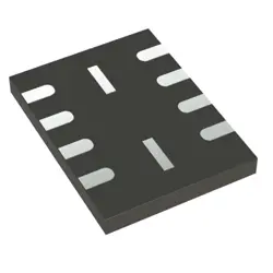
Изображения являются только для ссылки
TC74VHC541FT
+БОМBuffers & Line Drivers Lo-Volt Buffer
-
ПроизводительТошиба
-
Мфр. Часть #TC74VHC541FT
-
Лист данных TC74VHC541FT DataSheet
-
В наличии10428
365 Дни гарантии качества
7*24 часы обслуживания каранти
90-гарантия послепродажного дня
Гарантия подлинного продукта
Спецификации
| Атрибут | Ценность |
| Standard Pack Qty | 2000 |
Обзор
Description
Key features include:
- High-speed operation with typical propagation delay of 4.5 ns at 5V.
- 3-state outputs for easy bus interfacing.
- Low quiescent current consumption, enhancing power efficiency.
- Wide operating temperature range, suitable for various environments.
The TC74VHC541FT is typically packaged in a TSSOP (Thin Shrink Small Outline Package), making it suitable for compact circuit designs. Its robust performance and versatile utility make it an excellent choice for modern electronic applications.
Equivalent
Features
1. High-Speed Operation: It offers fast signal processing with a typical propagation delay time of 4.7 ns at V_CC = 5V.
2. Wide Operating Voltage Range: Compatible with a broad voltage range from 2V to 5.5V, making it versatile for various applications.
3. Low Power Consumption: Designed for reduced power usage with a low static power dissipation.
4. 3-State Outputs: Provides the ability to connect multiple outputs to a common bus line, aiding in flexible design configurations.
5. Balanced Propagation Delays: Ensures uniform signal timing across all outputs.
6. High Output Drive Capability: Can drive 50pF loads, suitable for driving standard TTL loads.
7. Input and Output Protection: Includes protection against static discharge and latch-up, enhancing device reliability.
These features make the TC74VHC541FT suitable for buffering and driving signals in digital circuits, particularly where high-speed and low-power operations are required.
Pinout
The device has a total of 20 pins. The key functions of these pins are as follows:
- Pins 1 and 19 (OE1 and OE2): Output Enable inputs, active-low. These control the 3-state outputs. The outputs are enabled when these pins are held low.
- Pins 2 to 9 (A1 to A8): Data inputs. These are the inputs for the eight channels of the device.
- Pins 18 to 11 (Y1 to Y8): Data outputs. These are the outputs for the eight channels, and they reflect the input data when the output is enabled.
- Pin 10 (GND): Ground.
- Pin 20 (VCC): Supply voltage.
This device is commonly used for driving bus lines and is suitable for a wide range of applications requiring high-speed data transmission.