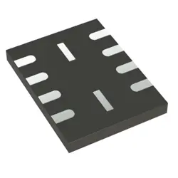
Изображения являются только для ссылки
TLV9302IDR
+БОМ-
ПроизводительТехасские инструменты
-
Мфр. Часть #TLV9302IDR
-
В наличии5359
365 Дни гарантии качества
7*24 часы обслуживания каранти
90-гарантия послепродажного дня
Гарантия подлинного продукта
Спецификации
| Атрибут | Ценность |
| Package | Tape & Reel (TR),Cut Tape (CT) |
| ProductStatus | Active |
| AmplifierType | General Purpose |
| NumberofCircuits | 2 |
| OutputType | Rail-to-Rail |
| SlewRate | 3V/µs |
| GainBandwidthProduct | 1 MHz |
| Current-InputBias | 10 pA |
| Voltage-InputOffset | 500 µV |
| Current-Supply | 150µA (x2 Channels) |
| Current-Output/Channel | 60 mA |
| Voltage-SupplySpan(Min) | 4.5 V |
| Voltage-SupplySpan(Max) | 40 V |
| OperatingTemperature | -40°C ~ 125°C (TA) |
| MountingType | Surface Mount |
| Package/Case | 8-SOIC (0.154, 3.90mm Width) |
Обзор
Description
The TLV9302IDR is a dual operational amplifier from Texas Instruments, known for its low power consumption and wide bandwidth. It operates on a supply voltage range from 2.7 V to 6 V, making it suitable for a variety of applications. This op-amp features rail-to-rail input and output, ensuring maximum dynamic range in low-voltage systems. It has a gain bandwidth product of 3 MHz, which allows for precise and accurate signal amplification in high-frequency applications.
The TLV9302IDR is designed for use in environments requiring low-noise performance with its low input bias current. Its small form factor, provided in an 8-pin SOIC package, is ideal for space-constrained applications. Key features include a low quiescent current of 550 µA per amplifier and an operating temperature range from -40°C to 125°C, making it versatile for both industrial and consumer electronics.
Applications commonly utilizing the TLV9302IDR include sensor signal conditioning, medical instrumentation, and portable devices, where efficient power usage and reliable performance are crucial.
The TLV9302IDR is designed for use in environments requiring low-noise performance with its low input bias current. Its small form factor, provided in an 8-pin SOIC package, is ideal for space-constrained applications. Key features include a low quiescent current of 550 µA per amplifier and an operating temperature range from -40°C to 125°C, making it versatile for both industrial and consumer electronics.
Applications commonly utilizing the TLV9302IDR include sensor signal conditioning, medical instrumentation, and portable devices, where efficient power usage and reliable performance are crucial.
Equivalent
The TLV9302IDR is a dual operational amplifier from Texas Instruments. Equivalent products could include the LM358 from Texas Instruments, the MCP6002 from Microchip Technology, and the NJM4558 from New Japan Radio (NJR). These are all dual op-amps with comparable general-purpose characteristics, though specific parameters may vary, so it's essential to verify compatibility based on your application needs.
Features
The TLV9302IDR is a dual-channel operational amplifier (op-amp) from Texas Instruments, designed for precision applications. Key features include:
1. Low Offset Voltage: Offers low offset voltage, enhancing accuracy in signal processing tasks.
2. Wide Supply Voltage Range: Operates effectively across a wide supply voltage range, from 2.7V to 16V, making it versatile for various applications.
3. Low Noise: Provides low input noise, suitable for precision measurements.
4. Rail-to-Rail Output: Ensures maximum output voltage swing, improving dynamic range.
5. High Slew Rate: Features a slew rate of 5 V/µs, enabling fast response times.
6. Unity-Gain Bandwidth: Offers a bandwidth of 3 MHz, allowing it to handle a range of frequencies.
7. Low Power Consumption: Designed for low power consumption, ideal for battery-powered devices.
8. Small Package: Available in a small package, such as the SOIC-8, facilitating compact circuit designs.
9. Temperature Range: Operates across a wide temperature range, supporting use in various environmental conditions.
These features make the TLV9302IDR suitable for applications in industrial, automotive, and consumer electronics.
1. Low Offset Voltage: Offers low offset voltage, enhancing accuracy in signal processing tasks.
2. Wide Supply Voltage Range: Operates effectively across a wide supply voltage range, from 2.7V to 16V, making it versatile for various applications.
3. Low Noise: Provides low input noise, suitable for precision measurements.
4. Rail-to-Rail Output: Ensures maximum output voltage swing, improving dynamic range.
5. High Slew Rate: Features a slew rate of 5 V/µs, enabling fast response times.
6. Unity-Gain Bandwidth: Offers a bandwidth of 3 MHz, allowing it to handle a range of frequencies.
7. Low Power Consumption: Designed for low power consumption, ideal for battery-powered devices.
8. Small Package: Available in a small package, such as the SOIC-8, facilitating compact circuit designs.
9. Temperature Range: Operates across a wide temperature range, supporting use in various environmental conditions.
These features make the TLV9302IDR suitable for applications in industrial, automotive, and consumer electronics.
Pinout
The TLV9302IDR is a dual operational amplifier (op-amp) from Texas Instruments. It comes in an 8-pin SOIC (Small Outline Integrated Circuit) package. Here is a brief overview of the pin functions:
1. Pin 1 (OUT1): Output of the first operational amplifier.
2. Pin 2 (IN–1): Inverting input of the first operational amplifier.
3. Pin 3 (IN+1): Non-inverting input of the first operational amplifier.
4. Pin 4 (V– or GND): Negative power supply or ground.
5. Pin 5 (IN+2): Non-inverting input of the second operational amplifier.
6. Pin 6 (IN–2): Inverting input of the second operational amplifier.
7. Pin 7 (OUT2): Output of the second operational amplifier.
8. Pin 8 (V+): Positive power supply.
The TLV9302IDR is designed for general-purpose applications and supports a wide range of input common-mode voltages, making it versatile for different circuits. It is often used in signal conditioning, filtering, or as a buffer in various electronic applications.
1. Pin 1 (OUT1): Output of the first operational amplifier.
2. Pin 2 (IN–1): Inverting input of the first operational amplifier.
3. Pin 3 (IN+1): Non-inverting input of the first operational amplifier.
4. Pin 4 (V– or GND): Negative power supply or ground.
5. Pin 5 (IN+2): Non-inverting input of the second operational amplifier.
6. Pin 6 (IN–2): Inverting input of the second operational amplifier.
7. Pin 7 (OUT2): Output of the second operational amplifier.
8. Pin 8 (V+): Positive power supply.
The TLV9302IDR is designed for general-purpose applications and supports a wide range of input common-mode voltages, making it versatile for different circuits. It is often used in signal conditioning, filtering, or as a buffer in various electronic applications.
Manufacturer
The TLV9302IDR is manufactured by Texas Instruments Incorporated (TI). Texas Instruments is a global semiconductor company that designs and manufactures a wide range of electronic components, including integrated circuits, microcontrollers, and sensors. The company serves various industries such as automotive, industrial, personal electronics, communications equipment, and enterprise systems. TI is known for its innovation and significant contributions to the fields of analog and embedded processing technologies.
Application
The TLV9302IDR is a dual operational amplifier suitable for various applications. It is commonly used in sensor signal conditioning, data acquisition systems, and active filtering due to its low noise and low power consumption. The amplifier is also ideal for medical instrumentation and portable devices, thanks to its wide supply voltage range and small package size. Additionally, the TLV9302IDR is used in audio processing, battery-powered applications, and industrial process controls, benefiting from its stability and precision.
Package
The TLV9302IDR is an operational amplifier from Texas Instruments, available in an 8-pin SOIC (Small Outline Integrated Circuit) package type.