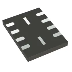
Изображения являются только для ссылки
10M02SCE144A7G
+БОМIC FPGA 101 I/O 144EQFP
-
ПроизводительАльтера
-
Мфр. Часть #10M02SCE144A7G
-
В наличии4832
365 Дни гарантии качества
7*24 часы обслуживания каранти
90-гарантия послепродажного дня
Гарантия подлинного продукта
Спецификации
| Атрибут | Ценность |
| Series | MAX® 10 |
| PartStatus | Active |
| DigiKeyProgrammable | Not Verified |
| NumberofLogicElements/Cells | 2000 |
| TotalRAMBits | 110592 |
| NumberofI/O | 101 |
| Voltage-Supply | 2.85V ~ 3.465V |
| MountingType | Surface Mount |
| OperatingTemperature | -40°C ~ 125°C (TJ) |
| Package/Case | 144-LQFP Exposed Pad |
| SupplierDevicePackage | 144-EQFP (20x20) |
| NumberofLABs/CLBs | 125 |
Обзор
Description
The code "10M02SCE144A7G" appears to be a product or model identifier, likely related to electronics, machinery, or manufacturing components. The structure typically includes specifications about the product's series, version, or features. Here's a potential breakdown:
- 10M: May indicate a specific category or series of the product.
- 02: Could represent a version number or a model variation.
- SCE: Might denote a specific feature, standard, or technology type associated with the product.
- 144: Often relates to a technical specification, such as dimensions, capacity, or configuration.
- A7G: Generally represents additional features, revisions, or compliance codes.
Without more context, it's difficult to provide a precise introduction. For detailed information, it would be advisable to refer to the manufacturer's specifications or product documentation. If you have a specific industry or product type in mind, that could help narrow down the explanation further.
- 10M: May indicate a specific category or series of the product.
- 02: Could represent a version number or a model variation.
- SCE: Might denote a specific feature, standard, or technology type associated with the product.
- 144: Often relates to a technical specification, such as dimensions, capacity, or configuration.
- A7G: Generally represents additional features, revisions, or compliance codes.
Without more context, it's difficult to provide a precise introduction. For detailed information, it would be advisable to refer to the manufacturer's specifications or product documentation. If you have a specific industry or product type in mind, that could help narrow down the explanation further.
Equivalent
The 10M02SCE144A7G is a FPGA from Intel's MAX 10 series. Equivalent products include the 10M04SCE144A7G (higher logic elements) and 10M08SCE144A7G (even higher logic elements), which offer increased capacity. Other alternatives might come from similar FPGA families, like those from Lattice or Xilinx, but ensure to check the specific application requirements such as I/O count, power consumption, and performance metrics for compatibility.
Features
The 10M02SCE144A7G is a member of Intel's MAX 10 FPGA series, designed for a variety of applications including embedded systems, industrial automation, and telecommunications. Key features include:
1. Density: 2,000 logic elements, providing sufficient capacity for moderate complexity designs.
2. I/O: 144 pins with support for various I/O standards, enabling flexibility in interfacing.
3. Embedded Memory: Offers up to 64 Kbits of embedded memory, useful for data storage and buffering.
4. Power Efficiency: Operates at low power, making it suitable for battery-operated devices and energy-efficient applications.
5. Single Supply Voltage: Simplifies power design with a single supply voltage requirement.
6. Integrated Flash Memory: Supports in-system configuration and reconfiguration, enhancing flexibility.
7. Development Support: Compatible with Intel Quartus Prime software for design and implementation.
Overall, the 10M02SCE144A7G combines low power consumption with adequate resources for mid-range FPGA applications.
1. Density: 2,000 logic elements, providing sufficient capacity for moderate complexity designs.
2. I/O: 144 pins with support for various I/O standards, enabling flexibility in interfacing.
3. Embedded Memory: Offers up to 64 Kbits of embedded memory, useful for data storage and buffering.
4. Power Efficiency: Operates at low power, making it suitable for battery-operated devices and energy-efficient applications.
5. Single Supply Voltage: Simplifies power design with a single supply voltage requirement.
6. Integrated Flash Memory: Supports in-system configuration and reconfiguration, enhancing flexibility.
7. Development Support: Compatible with Intel Quartus Prime software for design and implementation.
Overall, the 10M02SCE144A7G combines low power consumption with adequate resources for mid-range FPGA applications.
Pinout
The 10M02SCE144A7G is an FPGA (Field-Programmable Gate Array) from Intel's MAX 10 series. It has a pin count of 144 pins.
The functions of these pins include:
1. I/O Pins: Configurable for input, output, or bidirectional data communication.
2. Power Supply Pins: For supplying the core and I/O power.
3. Ground Pins: For grounding the device.
4. Clock Pins: For providing external clock signals.
5. Configuration Pins: For programming the FPGA, including JTAG pins for in-system programming.
6. Dedicated Global Signal Pins: For clock and reset signals across the FPGA.
This part is designed for a variety of applications, including embedded systems, industrial control, and communication systems.
The functions of these pins include:
1. I/O Pins: Configurable for input, output, or bidirectional data communication.
2. Power Supply Pins: For supplying the core and I/O power.
3. Ground Pins: For grounding the device.
4. Clock Pins: For providing external clock signals.
5. Configuration Pins: For programming the FPGA, including JTAG pins for in-system programming.
6. Dedicated Global Signal Pins: For clock and reset signals across the FPGA.
This part is designed for a variety of applications, including embedded systems, industrial control, and communication systems.
Manufacturer
The 10M02SCE144A7G is manufactured by Intel Corporation, specifically under its Altera product line. Intel is a multinational technology company primarily known for designing and manufacturing semiconductor products, including microprocessors, integrated circuits, and FPGA (Field Programmable Gate Array) devices.
Altera, which was acquired by Intel in 2015, focuses on developing FPGAs, CPLDs (Complex Programmable Logic Devices), and related technologies, catering to various industries such as telecommunications, automotive, consumer electronics, and industrial applications.
Intel Corporation, headquartered in Santa Clara, California, is one of the largest and most influential players in the global semiconductor industry, known for its innovation in computing technologies and contributions to the development of modern computing architecture.
Altera, which was acquired by Intel in 2015, focuses on developing FPGAs, CPLDs (Complex Programmable Logic Devices), and related technologies, catering to various industries such as telecommunications, automotive, consumer electronics, and industrial applications.
Intel Corporation, headquartered in Santa Clara, California, is one of the largest and most influential players in the global semiconductor industry, known for its innovation in computing technologies and contributions to the development of modern computing architecture.
Application
The 10M02SCE144A7G is a low-power, 2,000 logic element FPGA (Field-Programmable Gate Array) from Intel (formerly Altera). It is used in various applications, including:
1. Embedded Systems: Custom processing and control functions.
2. Signal Processing: Real-time data manipulation in communication systems.
3. Consumer Electronics: Implementing interfaces and protocols.
4. Automotive: Sensor data processing and control systems.
5. Industrial Automation: Robotics and machine control.
6. IoT Devices: Enabling connectivity and local processing.
7. Prototyping: Rapid development of digital circuits.
This versatile FPGA supports various digital logic functions, making it suitable for a wide range of applications.
1. Embedded Systems: Custom processing and control functions.
2. Signal Processing: Real-time data manipulation in communication systems.
3. Consumer Electronics: Implementing interfaces and protocols.
4. Automotive: Sensor data processing and control systems.
5. Industrial Automation: Robotics and machine control.
6. IoT Devices: Enabling connectivity and local processing.
7. Prototyping: Rapid development of digital circuits.
This versatile FPGA supports various digital logic functions, making it suitable for a wide range of applications.
Package
The 10M02SCE144A7G is packaged in a 144-ball LFBGA (Low-Profile Fine-Pitch Ball Grid Array) format. This type of package is designed for efficient thermal performance and space-saving on PCBs, making it suitable for various applications in FPGAs and other integrated circuits.