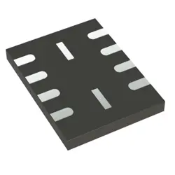
Изображения являются только для ссылки
MT29F1G08ABBEAH4:E
+БОМIC FLASH 1GBIT PARALLEL 63VFBGA
-
ПроизводительКомпания Micron Technology Inc.
-
Мфр. Часть #MT29F1G08ABBEAH4:E
-
В наличии9404
365 Дни гарантии качества
7*24 часы обслуживания каранти
90-гарантия послепродажного дня
Гарантия подлинного продукта
Спецификации
| Атрибут | Ценность |
| Part Status | Obsolete |
| DigiKey Programmable | Not Verified |
| Memory Type | Non-Volatile |
| Memory Format | FLASH |
| Technology | FLASH - NAND |
| Memory Size | 1Gbit |
| Memory Organization | 128M x 8 |
| Memory Interface | Parallel |
| Voltage - Supply | 1.7V ~ 1.95V |
| Operating Temperature | 0°C ~ 70°C (TA) |
| Mounting Type | Surface Mount |
| Package / Case | 63-VFBGA |
| Supplier Device Package | 63-VFBGA (9x11) |
| Base Product Number | MT29F1G08 |
Обзор
Description
The MT29F1G08ABBEAH4:E is a NAND flash memory chip manufactured by Micron Technology. It has a storage capacity of 1 gigabit (Gb), or 128 megabytes (MB), and is designed for high-performance applications in consumer electronics, mobile devices, and embedded systems. This chip uses multilevel cell (MLC) technology, allowing it to store multiple bits per cell, which enhances density and reduces cost per bit.
The device features a x8 data bus interface and operates on a supply voltage of 2.7V to 3.6V. It supports various functionalities, including random read/write, page program operations, and block erase capabilities, making it suitable for applications requiring speed and efficiency. The MT29F1G08ABBEAH4:E is also designed to be reliable, incorporating advanced error correction and wear leveling techniques to extend the lifespan of the memory. This NAND flash memory is commonly utilized in applications such as smartphones, tablets, and solid-state drives (SSDs), where compact and efficient storage solutions are essential.
The device features a x8 data bus interface and operates on a supply voltage of 2.7V to 3.6V. It supports various functionalities, including random read/write, page program operations, and block erase capabilities, making it suitable for applications requiring speed and efficiency. The MT29F1G08ABBEAH4:E is also designed to be reliable, incorporating advanced error correction and wear leveling techniques to extend the lifespan of the memory. This NAND flash memory is commonly utilized in applications such as smartphones, tablets, and solid-state drives (SSDs), where compact and efficient storage solutions are essential.
Equivalent
The MT29F1G08ABBEAH4:E chip is a NAND flash memory device. Equivalent products include:
1. Samsung K9GAG08U0M - 1Gb NAND Flash
2. Toshiba TH58NVG1S0H - 1Gb NAND Flash
3. SK Hynix H26M31001G - 1Gb NAND Flash
Ensure the specifications match, such as density, package type, and interface, for compatibility.
1. Samsung K9GAG08U0M - 1Gb NAND Flash
2. Toshiba TH58NVG1S0H - 1Gb NAND Flash
3. SK Hynix H26M31001G - 1Gb NAND Flash
Ensure the specifications match, such as density, package type, and interface, for compatibility.
Features
The MT29F1G08ABBEAH4:E is a 1 Gigabit (128MB) NAND Flash memory chip produced by Micron Technology. It features:
- Flash Type: NAND Flash, SLC (Single-Level Cell).
- Interface: OnFI (Open NAND Flash Interface) compatible.
- Voltage: Operates at a supply voltage of 2.7V to 3.6V.
- Access Time: Fast read and write speeds, typically optimized for high-performance applications.
- Endurance: Supports a high number of program/erase cycles, suitable for demanding applications.
- Package: Available in a compact 48-ball VFBGA (Very Fine Ball Grid Array) package for space-constrained designs.
- Applications: Commonly used in mobile devices, SSDs, and various consumer electronics for data storage.
This device is designed for reliable data retention and performance, making it ideal for embedded systems and other applications requiring efficient storage solutions.
- Flash Type: NAND Flash, SLC (Single-Level Cell).
- Interface: OnFI (Open NAND Flash Interface) compatible.
- Voltage: Operates at a supply voltage of 2.7V to 3.6V.
- Access Time: Fast read and write speeds, typically optimized for high-performance applications.
- Endurance: Supports a high number of program/erase cycles, suitable for demanding applications.
- Package: Available in a compact 48-ball VFBGA (Very Fine Ball Grid Array) package for space-constrained designs.
- Applications: Commonly used in mobile devices, SSDs, and various consumer electronics for data storage.
This device is designed for reliable data retention and performance, making it ideal for embedded systems and other applications requiring efficient storage solutions.
Pinout
The MT29F1G08ABBEAH4:E is a NAND flash memory device with a pin count of 48 pins. This device features a variety of functions, including data storage, memory management, and interface control. It operates using a NAND interface, which allows for high-speed memory transactions and efficient data handling.
Key functions include:
1. Data Input/Output: Pins for reading and writing data.
2. Chip Enable (CE): Activates the chip for operation.
3. Write Enable (WE): Initiates write operations.
4. Read Enable (RE): Starts read operations.
5. Ready/Busy (R/B): Indicates the status of the memory operation.
6. Address Inputs: Pins for addressing memory locations.
This device is designed for applications requiring high-density storage, such as mobile devices, tablets, and consumer electronics.
Key functions include:
1. Data Input/Output: Pins for reading and writing data.
2. Chip Enable (CE): Activates the chip for operation.
3. Write Enable (WE): Initiates write operations.
4. Read Enable (RE): Starts read operations.
5. Ready/Busy (R/B): Indicates the status of the memory operation.
6. Address Inputs: Pins for addressing memory locations.
This device is designed for applications requiring high-density storage, such as mobile devices, tablets, and consumer electronics.
Manufacturer
The manufacturer of the MT29F1G08ABBEAH4:E is Micron Technology, Inc. Micron is a leading American company that specializes in the production of memory and storage solutions, including DRAM, NAND flash memory, and other semiconductor technologies. Founded in 1978 and headquartered in Boise, Idaho, Micron plays a critical role in the global semiconductor industry, supplying memory products for various applications such as computing, mobile devices, automotive, and data centers. The company's focus on innovation and technology advancement has positioned it as a key player in the market, contributing to developments in high-performance memory solutions and storage technologies.
Application
The MT29F1G08ABBEAH4:E is a 1Gb NAND flash memory device primarily used in applications such as mobile devices, consumer electronics, embedded systems, and solid-state drives (SSDs). It provides high-density storage for smartphones, tablets, and digital cameras, enabling fast read and write operations. Additionally, it is suitable for industrial applications requiring reliable data storage and retrieval, such as automotive systems, IoT devices, and wearables. The device’s low power consumption and durability make it ideal for applications demanding efficient performance and longevity.
Package
The MT29F1G08ABBEAH4:E is packaged in a small, thin BGA (Ball Grid Array) format, specifically a 48-ball BGA package. This type of packaging is designed for high-density applications, providing efficient thermal and electrical performance.