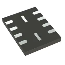
Изображения являются только для ссылки
S99FL164KMM13
+БОМIC FLASH NOR
-
Производителькорпорации Cypress Semiconductor Corp
-
Мфр. Часть #S99FL164KMM13
-
В наличии5331
365 Дни гарантии качества
7*24 часы обслуживания каранти
90-гарантия послепродажного дня
Гарантия подлинного продукта
Спецификации
| Атрибут | Ценность |
| Package / Case | Tape & Reel (TR) |
| Part Status | Obsolete |
Обзор
Description
The designation "S99FL164KMM13" appears to be a part number or a model identifier, potentially for a specific electronic component, semiconductor, or specialized device. These sequences are often used by manufacturers to uniquely identify products, allowing for precise specification, ordering, and inventory management. Such components are commonly used in various industries, including consumer electronics, automotive, telecommunications, and computing.
When examining a part number like "S99FL164KMM13," it's important to reference the manufacturer's datasheet or official documentation. This will provide detailed information about the component's specifications, including its electrical characteristics, packaging type, pin configuration, operational limits, and potential applications. Understanding these details is crucial for engineers and professionals who integrate such components into larger systems, ensuring compatibility and optimal performance.
Without specific context or associated documentation, it is challenging to provide detailed information about "S99FL164KMM13." If you are interested in this component, I recommend contacting the manufacturer directly or visiting their official website for more precise information and technical support.
When examining a part number like "S99FL164KMM13," it's important to reference the manufacturer's datasheet or official documentation. This will provide detailed information about the component's specifications, including its electrical characteristics, packaging type, pin configuration, operational limits, and potential applications. Understanding these details is crucial for engineers and professionals who integrate such components into larger systems, ensuring compatibility and optimal performance.
Without specific context or associated documentation, it is challenging to provide detailed information about "S99FL164KMM13." If you are interested in this component, I recommend contacting the manufacturer directly or visiting their official website for more precise information and technical support.
Equivalent
The S99FL164KMM13 is a serial flash memory chip produced by Cypress Semiconductor (now part of Infineon Technologies). Equivalent products could include similar NOR flash memory chips from manufacturers like Micron, Winbond, or Macronix, offering similar storage capacity, interface, and speed. The specific equivalents would depend on the required specifications like voltage, temperature range, and package type. Always check the datasheets for compatibility.
Features
The S99FL164KMM13 is a NOR Flash memory chip, often used in embedded systems for non-volatile storage. Here are some key features:
1. Architecture: It offers a 16 Mbit capacity organized in a 1M x 16-bit or 2M x 8-bit configuration.
2. Technology: Based on NOR Flash technology, providing fast random access times suitable for code execution.
3. Interface: Employs a parallel interface, allowing for efficient data transfer.
4. Voltage: Typically operates at a voltage range compatible with various systems, often around 3V.
5. Sector Architecture: Features sector-based architecture, allowing for flexible erase operations on specific memory segments.
6. Endurance: Supports a significant number of program/erase cycles, making it durable for repeated use.
7. Data Retention: Provides long-term data retention, generally for over a decade.
8. Security Features: May include features like block protection to prevent accidental data alteration.
These attributes make it suitable for applications requiring reliable, high-speed read operations, such as in firmware storage for electronic devices.
1. Architecture: It offers a 16 Mbit capacity organized in a 1M x 16-bit or 2M x 8-bit configuration.
2. Technology: Based on NOR Flash technology, providing fast random access times suitable for code execution.
3. Interface: Employs a parallel interface, allowing for efficient data transfer.
4. Voltage: Typically operates at a voltage range compatible with various systems, often around 3V.
5. Sector Architecture: Features sector-based architecture, allowing for flexible erase operations on specific memory segments.
6. Endurance: Supports a significant number of program/erase cycles, making it durable for repeated use.
7. Data Retention: Provides long-term data retention, generally for over a decade.
8. Security Features: May include features like block protection to prevent accidental data alteration.
These attributes make it suitable for applications requiring reliable, high-speed read operations, such as in firmware storage for electronic devices.
Pinout
The S99FL164KMM13 is a serial flash memory device, often used in electronics for data storage. It typically comes in a standard 8-pin package, which is common for serial flash memories. The primary functions of these pins include:
1. Chip Select (CS#): Activates the device.
2. Serial Data Input (SI/IO0): Inputs data into the device.
3. Serial Data Output (SO/IO1): Outputs data from the device.
4. Write Protect (WP#/IO2): Protects the device from write operations.
5. Hold (HOLD#/IO3): Pauses serial communication.
6. Serial Clock (SCK): Provides the clock pulses.
7. Ground (VSS): Connects to ground.
8. Power Supply (VCC): Powers the device.
These pins allow the device to interface with microcontrollers or other digital systems and enable operations like reading, writing, and erasing the memory contents. The 8-pin structure is designed for simplicity and compatibility with various applications requiring non-volatile memory storage.
1. Chip Select (CS#): Activates the device.
2. Serial Data Input (SI/IO0): Inputs data into the device.
3. Serial Data Output (SO/IO1): Outputs data from the device.
4. Write Protect (WP#/IO2): Protects the device from write operations.
5. Hold (HOLD#/IO3): Pauses serial communication.
6. Serial Clock (SCK): Provides the clock pulses.
7. Ground (VSS): Connects to ground.
8. Power Supply (VCC): Powers the device.
These pins allow the device to interface with microcontrollers or other digital systems and enable operations like reading, writing, and erasing the memory contents. The 8-pin structure is designed for simplicity and compatibility with various applications requiring non-volatile memory storage.
Manufacturer
The S99FL164KMM13 is a product manufactured by Infineon Technologies. Infineon is a German semiconductor manufacturer that designs, develops, manufactures, and markets a broad range of semiconductors and system solutions focusing on automotive, industrial power control, power management and multimarket, and digital security solutions. The company is known for its expertise in power semiconductors, microcontrollers, security controllers, radio-frequency products, sensors, and other semiconductors that are integral to the advancement of technology in various fields. Infineon is a key player in the global semiconductor industry and is recognized for its innovation and sustainability efforts in providing solutions tailored for energy efficiency, mobility, and security.
Application
The S99FL164KMM13 is a specific model of NOR Flash memory, commonly used in applications requiring non-volatile storage. Key application areas include embedded systems, where it stores firmware and system code, and consumer electronics like smartphones, tablets, and digital cameras for data storage. It's also used in automotive electronics for its reliability in harsh environments, and in industrial automation systems for logging data and maintaining configuration settings. Its fast read times and endurance make it suitable for applications needing frequent read operations. Additionally, it's employed in networking equipment, medical devices, and any system requiring secure and persistent data storage.
Package
The package type for the S99FL164KMM13 is generally a BGA (Ball Grid Array) package. BGAs are commonly used for their high lead count capability and efficient use of space on printed circuit boards. However, please verify with the specific manufacturer datasheet for precise information, as variations could exist.