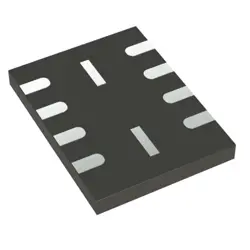
Изображения являются только для ссылки
ADP3654ARDZ
+БОМIC MOSFET DVR 4A DUAL HS 8SOIC
-
ПроизводительКомпания Analog Devices Inc.
-
Мфр. Часть #ADP3654ARDZ
-
Лист данных ADP3654ARDZ DataSheet
-
Пакет SOP8
-
В наличии3719
365 Дни гарантии качества
7*24 часы обслуживания каранти
90-гарантия послепродажного дня
Гарантия подлинного продукта
Спецификации
| Атрибут | Ценность |
| Package | Tube |
| ProductStatus | Active |
| DrivenConfiguration | Low-Side |
| ChannelType | Independent |
| NumberofDrivers | 2 |
| GateType | N-Channel MOSFET |
| Voltage-Supply | 4.5V ~ 18V |
| LogicVoltage-VILVIH | 0.8V, 2V |
| Current-PeakOutput(SourceSink) | 4A, 4A |
| InputType | Non-Inverting |
| Rise/FallTime(Typ) | 10ns, 10ns |
| OperatingTemperature | -40°C ~ 125°C (TJ) |
| MountingType | Surface Mount |
| Package/Case | 8-SOIC (0.154, 3.90mm Width) Exposed Pad |
Обзор
Description
In general, if ADP3654ARDZ pertains to an electronic component, it could be part of a power management system, sensor, or integrated circuit—common roles for components in such domains. It might be produced by a well-known manufacturer or company specializing in technology or electronics.
To understand its specific purpose or features, one would typically consult the manufacturer's datasheet or product documentation. These resources provide detailed specifications, including electrical characteristics, pin configurations, and application recommendations. For up-to-date and reliable information, checking the manufacturer's website or contacting their support for technical documentation is recommended. If ADP3654ARDZ is relevant in a particular niche or industry, community forums or technical support groups can also be valuable resources for insights and advice.
Equivalent
Features
1. High Efficiency: Optimized for high-frequency applications, leading to improved efficiency.
2. Dual Driver: Capable of driving both high-side and low-side N-channel MOSFETs.
3. Bootstrap Circuitry: Integrated bootstrap diode simplifies design and reduces component count.
4. Fast Switching: Features short propagation delay and fast rise/fall times enhancing performance in high-frequency applications.
5. Wide Supply Range: Operates from a wide supply voltage range, typically enhancing flexibility in various applications.
6. Under-Voltage Lockout (UVLO): Protects the MOSFETs by not allowing operation under unsafe conditions.
7. Thermal Protection: Includes thermal shutdown to prevent overheating.
8. Compact Package: Available in small packaging, ideal for space-constrained applications.
These features make it suitable for DC-DC converters, power supply modules, and various high-efficiency power management applications.
Pinout
The pinout of the ADP3654ARDZ includes:
1. VDD: Power supply input for the driver.
2. INA: Input control signal for the high-side MOSFET driver.
3. INB: Input control signal for the low-side MOSFET driver.
4. PGND: Ground connection for the power side.
5. OUTA: Output for driving the high-side MOSFET gate.
6. OUTB: Output for driving the low-side MOSFET gate.
7. NC (or no connect): This pin is not connected internally.
8. VCC: Logic supply voltage for the input side.
The ADP3654ARDZ is essential for ensuring efficient switching, reducing power loss, and improving the overall performance of power management systems.